Domestic specialists have managed to stabilize hexagonal silicon. The new material increases the conductivity and efficiency of transistors, opening up new horizons for Russian microelectronics.
Scientists at Lobachevsky University have developed a film containing silicon in the hexagonal phase. The new material can increase the efficiency of transistors, providing more current with a lower supply voltage. This discovery helps improve the characteristics of key components of integrated circuits and increase the productivity of microprocessors, according to the official website of the Decade of Science and Technology in Russia.
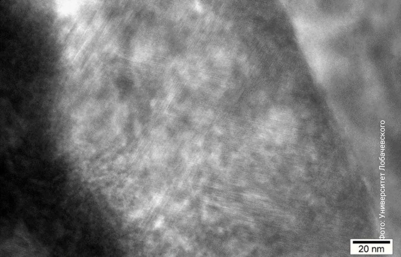
Silicon in the hexagonal phase has a unique crystalline structure, due to which the conductivity of the material in certain directions increases significantly. This contributes to an increase in electric current. There is one “but”: such structures are traditionally unstable and easily transform into the usual form of silicon. Domestic scientists have managed to successfully stabilize the hexagonal phase, opening up the prospect of wide industrial application of hexagonal silicon, clarifies Anton Konakov, Associate Professor of the Department of Quantum and Neuromorphic Technologies of the Physics Department of Lobachevsky University.
The new material is obtained by growing it on a substrate of ordinary silicon and then applying a top layer of germanium. Between them, a continuous and uniform layer of silicon in the hexagonal phase is formed. This technology allows creating films suitable for covering large areas of microcircuits with many contacts. The scientists intend to optimize and scale up their development for its further implementation in the Russian silicon microelectronics industry.
“In addition to the technologies for creating the hexagonal phase of silicon, we have managed to develop a number of original systems for growing thin films of silicon and germanium. These solutions are also patented. They can be used to create a wide range of materials, for example, to create a variety of thin-film structures used in the microelectronics industry,” concludes the author of the development, Associate Professor of the Department of Physics of Semiconductors, Electronics and Nanoelectronics of the Physics Department of Lobachevsky University, Nikolay Krivulin.